Semiconductor Grinding, Lapping, & Polishing Systems

Grind "2" CMP - The Journey!

Introduction
The capability to quickly and efficiently produce quality wafer surfaces in pilot line and R & D applications is key in today’s rapidly changing semiconductor environment. The engineers at Engis have developed a grind straight to polish process to meet these challenges for most compound semiconductor materials should that be bulk wafer or back thinning applications. Follow the process in our virtual exhibit and see how Engis can assist you in your processing challenges.
Stock Removal and Nano Grinding
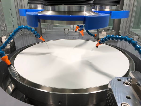
By adopting a stock removal and or nano grinding approach, surface roughness figures of 2nm Ra can be achieved therefore facilitating the capability to go straight to CMP after grinding. Watch Video!
No video selected
Select a video type in the sidebar.
CMP Chemical Mechanical Polishing
Post-Grinding Engis offers specifically developed machines and consumable products capable of efficiently producing Epi surfaces on virtually all semiconductor materials.
Semiconductor Wafer Grinding & Back Thinning
- SiC
- Si
- AI203
- GaN
- GaAs
- InP
- AIN
- Others

The CMP Process! Download TDS, Case Studies & Watch Videos
Grinder Video
Technical Data Specs
CaseStudy
BG & Polishing of InP Wafer
6" 4H SiC Grinding to CMP
InP Back Thinning Process
Products and Services
- We offer Products, Service and Technical Support
- Lapping and Polishing Systems
- FastLap Machines
- HYPREZ Slurries and Diamond Compounds
- Polishing Pads
